Chip-Off, ISP and Monolithic Flash Recovery
Removing or reading NAND chips directly is an acquisition method, not a complete recovery method — the controller’s ECC, scrambling and translation still have to be reversed before the dump means anything.
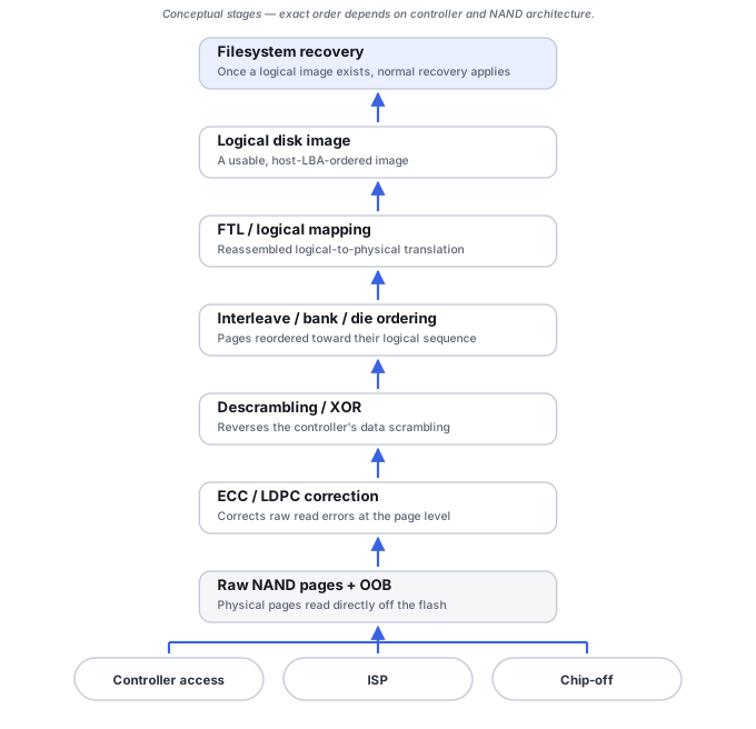
What chip-off actually means
In flash recovery, chip-off typically covers five distinct steps: remove the NAND package (or packages) from the circuit board, clean and prepare the package for reading, read the physical NAND through a compatible reader or adapter, save the raw physical dumps, and then reconstruct the controller's transformations in software before the result resembles a normal disk image. The acquisition step — physically getting bits off the chip — is often the easy part. The reconstruction step, covered below, is frequently the harder one.
When direct NAND access is actually worth considering
Chip-off tends to make sense when the NAND lives in a separate, identifiable package with a known pinout, when the NAND protocol involved is one a reader supports, when the controller's page layout and transformations are known or reversible, and when encryption does not block reconstruction of plaintext sectors. It tends to make less sense as a first move when the controller can still expose a stable logical view — see SSD Firmware, Translator and Controller-Level Recovery for why controller-aware access is often the better route on modern SSDs specifically.
ISP: reading NAND without removing it
In-system programming (ISP) style access reads the memory while it stays soldered to the board or module, by connecting to the relevant NAND signals through test points rather than desoldering the package. This can avoid the heat and mechanical risk of package removal and is sometimes the only option for monolithic devices with no discrete package to remove at all. ISP is not automatically easier than chip-off: it still requires the correct pinout and test points, isolating or resetting the original controller so it does not contend with the reader on the same bus, correct signal voltage, working signal integrity, and an understanding of chip-enable, ready/busy, read-enable, write-enable and data line behavior. ISP changes how the NAND is acquired; it does not remove the need to reconstruct the controller's logical mapping afterward.
Monolithic devices: no chip to remove
A monolithic device integrates the controller and NAND functions into one physical package or module — common in many microSD cards, compact USB flash drives and some embedded flash designs — so there may be no separate TSOP or BGA NAND package to lift off at all. Working with these can involve removing a protective coating or solder mask, locating test points, X-ray or internal-layout analysis, logic-analyzer work to identify the NAND bus signals, and controlled micro-soldering to make contact. This is specialist, model-specific work rather than a generic technique, and it is one reason monolithic USB sticks and memory cards get treated as a harder recovery class than devices with a removable NAND package.
Preserve raw pages and the spare/OOB area in full
Raw NAND pages typically carry a spare or out-of-band (OOB) area in addition to the user-data payload, holding fields related to ECC, bad-block markers, controller metadata, and sequence or block numbering. Acquisition that discards this spare-area data to save space can make reconstruction substantially harder or impossible later, since some of the information needed to reassemble the logical drive lives there rather than in the payload bytes. Preserve the complete raw page structure — payload and spare area together — during any physical NAND acquisition.
ECC, LDPC and read-retry are part of getting a usable dump
Raw NAND accumulates bit errors, and a raw page read outside the original controller path is not automatically error-corrected data. Reconstruction may need to determine codeword boundaries, identify the ECC scheme in use, correct bit errors, distinguish correctable pages from uncorrectable ones, and reread marginal pages using different read thresholds or retry strategies. Older, simpler NAND commonly used simpler ECC families; modern high-density TLC and QLC increasingly relies on stronger correction such as LDPC, which can require soft-information or vendor-specific read behavior rather than a single-pass dump. A raw acquisition should not be assumed to already be a clean, final source; acquisition quality itself can require iterative correction.
Descrambling and XOR are not the same problem as encryption
Flash controllers frequently transform data before programming it to NAND — commonly called scrambling or XOR — to improve bit-pattern characteristics or satisfy the controller's own implementation requirements. This can make a raw dump look pseudo-random even when the user never enabled any encryption at all. A known controller-specific scrambling pattern is typically reversible once identified, which is a fundamentally different situation from user or controller-level encryption that requires the correct key. Random-looking raw NAND, on its own, does not prove the drive was encrypted.
Interleave, bank and chip assembly
Controllers commonly distribute data across multiple NAND packages, dies, planes, chip-enable lines, channels or banks for performance, and reconstruction has to reverse that distribution — establishing chip order, bank order, page interleave, plane split/join and block pairing — before the dumps mean anything as a sequential address space. Multiple NAND dumps generally cannot be concatenated by file size or physical position and expected to produce the logical drive; they have to be joined according to the controller's own interleave scheme.
When encryption blocks chip-off outright
Many controllers apply transparent internal encryption as part of normal operation, in some cases regardless of whether the user ever configured a password. When the encryption key is tied to state the original controller managed internally, a raw NAND dump can be electrically complete and still cryptographically useless without that key or controller state — one of the main reasons chip-off can fail on a modern SSD even when every NAND package reads cleanly.
Why controller-specific access can beat chip-off on modern SSDs
Direct NAND recovery tends to be more straightforward on simpler controller architectures — older or simpler USB drives and memory cards are comparatively good chip-off candidates. Modern SSDs, with heavier ECC/LDPC, more aggressive scrambling, and often transparent encryption, more often benefit from controller-aware access when a supported route exists, because the working controller already performs the ECC correction, translation and descrambling that a chip-off workflow would otherwise have to reverse from scratch.
Raw NAND acquisition is only useful to the extent the controller's own behavior can be reconstructed afterward. Acquiring the chips is rarely the hard part; reversing what the controller did to the data before it reached them usually is.
Related: Flash Translation Layers and NAND Mapping · SSD Firmware, Translator and Controller-Level Recovery · Flash and SSD Controller Recovery Tools · USB Flash Drive Failure · When Software Recovery Is No Longer Appropriate